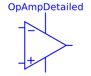
modelOpAmpDetailed
Detailed model of an operational amplifier
Information
The OpAmpDetailed model is a general operational amplifier model. The emphasis is on separating each important data sheet parameter into a sub-circuit independent of the other parameters. The model is broken down into five functional stages input, frequency response, gain, slew rate and an output stage. Each stage contains data sheet parameters to be modeled. This partitioning and the modelling of the separate submodels are based on the description in [Conelly1992].
Using [Conelly1992] Joachim Haase (Fraunhofer Institute for Integrated Circuits, Design Automation Division) transferred 2001 operational amplifier models into VHDL-AMS. Now one of these models, the model "amp(macro)" was transferred into Modelica.
Parameters
| Type | Name | Default | Description |
|---|
| SI.Resistance | Rdm | 2.0e6 | Input resistance (differential input mode) |
| SI.Resistance | Rcm | 2.0e9 | Input resistance (common mode) |
| SI.Capacitance | Cin | 1.4e-12 | Input capacitance |
| SI.Voltage | Vos | 1.0e-3 | Input offset voltage |
| SI.Current | Ib | 80.0e-9 | Input bias current |
| SI.Current | Ios | 20.0e-9 | Input offset current |
| SI.Voltage | vcp | 0.0 | Correction value for limiting by p_supply |
| SI.Voltage | vcm | 0.0 | Correction value for limiting by msupply |
| Real | Avd0 | 106.0 | Differential amplifier [dB] |
| Real | CMRR | 90.0 | Common-mode rejection [dB] |
| SI.Frequency | fp1 | 5.0 | Dominant pole |
| SI.Frequency | fp2 | 2.0e6 | Pole frequency |
| SI.Frequency | fp3 | 20.0e6 | Pole frequency |
| SI.Frequency | fp4 | 100.0e6 | Pole frequency |
| SI.Frequency | fz | 5.0e6 | Zero frequency |
| SI.VoltageSlope | sr_p | 0.5e6 | Slew rate for increase |
| SI.VoltageSlope | sr_m | 0.5e6 | Slew rate for decrease |
| SI.Resistance | Rout | 75.0 | Output resistance |
| SI.Current | Imaxso | 25.0e-3 | Maximal output current (source current) |
| SI.Current | Imaxsi | 25.0e-3 | Maximal output current (sink current) |
| SI.Time | Ts | 0.0000012 | Sampling time |
| SI.Voltage | vcp_abs | abs(vcp) | Positive correction value for limiting by p_supply |
| SI.Voltage | vcm_abs | abs(vcm) | Positive correction value for limiting by msupply |
| SI.Current | I1 | Ib + Ios/2.0 | Current of internal source I1 |
| SI.Current | I2 | Ib - Ios/2.0 | Current of internal source I2 |
| Real | Avd0_val | 10.0^(Avd0/20.0) | Differential mode gain |
| Real | Avcm_val | (Avd0_val/(10.0^(CMRR/20.0)))/2.0 | Common mode gain |
| SI.VoltageSlope | sr_p_val | abs(sr_p) | Value of slew rate for increase |
| SI.VoltageSlope | sr_m_val | -abs(sr_m) | Negative value of slew rate for increase |
| SI.Current | Imaxso_val | abs(Imaxso) | Orientation out outp |
| SI.Current | Imaxsi_val | abs(Imaxsi) | Orientation into outp |
Contents
| Name | Description |
|---|
 FCNiout_limit FCNiout_limit | Internal limitation function |
 FCNq_sum_limit FCNq_sum_limit | Internal limitation function |
Revisions
- June 17, 2009
- by Susann Wolf initially implemented