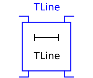
modelTLine
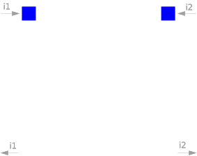
Extends from Modelica.Electrical.Analog.Interfaces.TwoPort (Component with two electrical ports, including current).
Information
Lossless transmission line with characteristic impedance Z0 and transmission delay TD. The lossless transmission line TLine is a two Port. Both port branches consist of a resistor with characteristic impedance Z0 and a controlled voltage source that takes into consideration the transmission delay TD. For further details see [Branin1967]. The model parameters can be derived from inductance and capacitance per length (L' resp. C'), i. e. Z0 = sqrt(L' / C').
There are three possibilities for specifying the transmission delay TD:
- Calculate TD = sqrt(L' * C')*length_of_line.
- Specify the normalized length NL, i.e. the length of the line divided by the wavelength corresponding to the frequency F: TD = NL / F.
- Specify NL = 1/4, i.e. the length of the line is assumed to be equal to a quarter of the wavelength corresponding to the frequency F: TD = 1/4 / F. In that case, the characteristic impedance Z0 is called natural impedance.
Resistance R' and conductance G' per meter are assumed to be zero.
References: [Branin1967], [Hoefer1985]
Parameters
| Type | Name | Default | Description |
|---|---|---|---|
| Modelica.Units.SI.Resistance | Z0 | Characteristic impedance | |
| Modelica.Units.SI.Time | TD | 0 | Transmission delay: specify > 0 if F and NL are not given |
| Modelica.Units.SI.Frequency | F | 0 | Frequency: specify > 0 if TD is not given |
| Real | NL | 1/4 | Normalized length: specify if TD is not given |
Connectors
| Type | Name | Default | Description |
|---|---|---|---|
| PositivePin | p1 (from FourPin) | Positive electrical pin of port 1 | |
| NegativePin | n1 (from FourPin) | Negative electrical pin of port 1 | |
| PositivePin | p2 (from FourPin) | Positive electrical pin of port 2 | |
| NegativePin | n2 (from FourPin) | Negative electrical pin of port 2 |
Components
| Type | Name | Default | Description |
|---|---|---|---|
| SI.Voltage | v1 (from FourPin) | Voltage drop of port 1 (= p1.v - n1.v) | |
| SI.Voltage | v2 (from FourPin) | Voltage drop of port 2 (= p2.v - n2.v) | |
| SI.Current | i1 (from FourPin) | Current flowing from pos. to neg. pin of port 1 | |
| SI.Current | i2 (from FourPin) | Current flowing from pos. to neg. pin of port 2 | |
| Modelica.Units.SI.Voltage | es | Voltage source of forward travelling wave | |
| Modelica.Units.SI.Voltage | er | Voltage source of reflected wave |
Revisions
- 1998
by Joachim Haase
initially implemented